


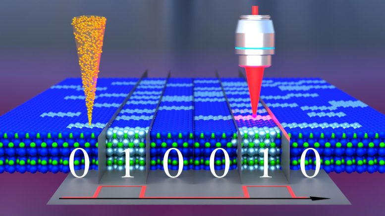
Information is written into optically active atomic defects by a focused ion beam (left) and read using cathodoluminescence or photoluminescence (right). Credit: M. Hollenbach, H. Schultheis
The team presents a new path to long-term data storage based on atomic-scale defects.
With the development of the Internet, social media, and cloud computing, the amount of data created around the world every day is rapidly increasing. This requires new technologies that can provide higher storage densities combined with secure long-term data archiving that far exceeds the capabilities of traditional data storage devices.An international research team led by Helmholtz – Zentrum Dresden – Rossendorf (HZDR) is currently proposing a new concept for long-term data storage based on atomic-scale defects in the semiconductor material silicon carbide. These defects are generated by a focused ion beam, allowing for high spatial resolution, fast write speeds, and low energy to store a single bit, the research team reports in the journal Advanced functional materials.
The latest estimates assume that around 330 million terabytes of new data are created every day, with 90% of the world's data generated in the past two years alone. Even though the sheer numbers already indicate the need for advanced data storage technologies, that is not the only issue associated with this development. “Current storage media have limited retention periods, so data must be migrated within a few years to avoid data loss. The energy consumption increases significantly, since a large amount of energy is consumed in the process,” said Dr. Georgy Astakhov from the HZDR Institute of Ion Beam Physics and Materials Research.
To alleviate this impending crisis, Astakhov's team is now introducing a new concept for long-term data storage based on atomic-scale defects in silicon carbide. These defects are triggered by a focused beam of protons or helium ions and read using a light emission mechanism associated with the defect.
Traditional storage devices are throttled due to physical effects
Magnetic memory is currently the first choice for high-capacity data storage solutions, but the laws of physics place limits on the storage density that can be achieved. To increase the size of magnetic particles, the size of the magnetic particles must be decreased. But then thermal fluctuations and diffusion processes within the material become important, exacerbating the impact on storage time. Tuning the magnetic properties of the material could potentially reduce this effect, but at the cost of more energy to store the information. Similarly, the performance of optical devices is also hampered by the laws of physics. The so-called diffraction limit places a limit on the size of the smallest recording bit, which cannot be smaller than half the wavelength of light, and sets a limit on the maximum storage capacity. The solution is multidimensional optical recording.
Silicon carbide is characterized by atomic-scale defects, particularly the absence of silicon atoms at lattice sites. The defects are created by a focused proton or helium ion beam, providing high spatial resolution, fast writing speeds, and low energy for storing single bits. “The diffraction limit of storage density inherent in optical media applies in our case as well. We overcome it by a 4D encoding scheme, where three spatial dimensions and an additional fourth The intensity dimension of is achieved by controlling the lateral position and depth as well as the number of defects. Photoluminescence caused by optical excitation is then exploited to read out the stored data optically. Furthermore, using focused electron beam excitation that causes observable cathodoluminescence, the areal memory density can be significantly improved.'' Astakhov highlights some salient features of his method. Masu.
Preserve data across generations
Depending on the environmental conditions in which the medium is stored, the stored information could be knocked out of the flaw again, but scientists have good news considering the material. It takes several generations under ambient conditions,” says Astakhov. There's more. By using near-infrared laser excitation, advanced encoding techniques, and multilayer data storage, i.e. stacking up to 10 silicon carbide layers, the team achieved areal storage densities comparable to his Blu-ray discs. Switching to electron beam excitation instead of optical excitation for data readout, the limits achievable with this method are comparable to the areal storage densities of currently reported prototype magnetic tapes, but with shorter storage times and Energy consumption is high. .
Reference: “Ultra-long-term high-density data storage using atomic defects in SiC” M. Hollenbach, C. Kasper, D. Erb, L. Bischoff, G. Hlawacek, H. Kraus, W. Kada, T. Ohshima, M. Helm, S. Fusko, V. Jakonov, GV Astakhov, March 4, 2024. Advanced functional materials.
DOI: 10.1002/adfm.202313413
For this research, the Rossendorf scientists collaborated with the Julius-Maximilians-Universität Würzburg (Germany), the Jet Propulsion Laboratory, the California Institute of Technology (USA), the Japan Institute for Quantum and Radiological Science and Technology (Japan), and Tohoku University (Japan). collaborated with researchers. . The research team's conceptual approach is not limited to silicon carbide and can be extended to other materials with optically active defects, including 2D materials.